The Machine Works, So Why Did TSMC Wait? Notes on Supply Chained's Episode About High NA EUV and 12-Inch Masks
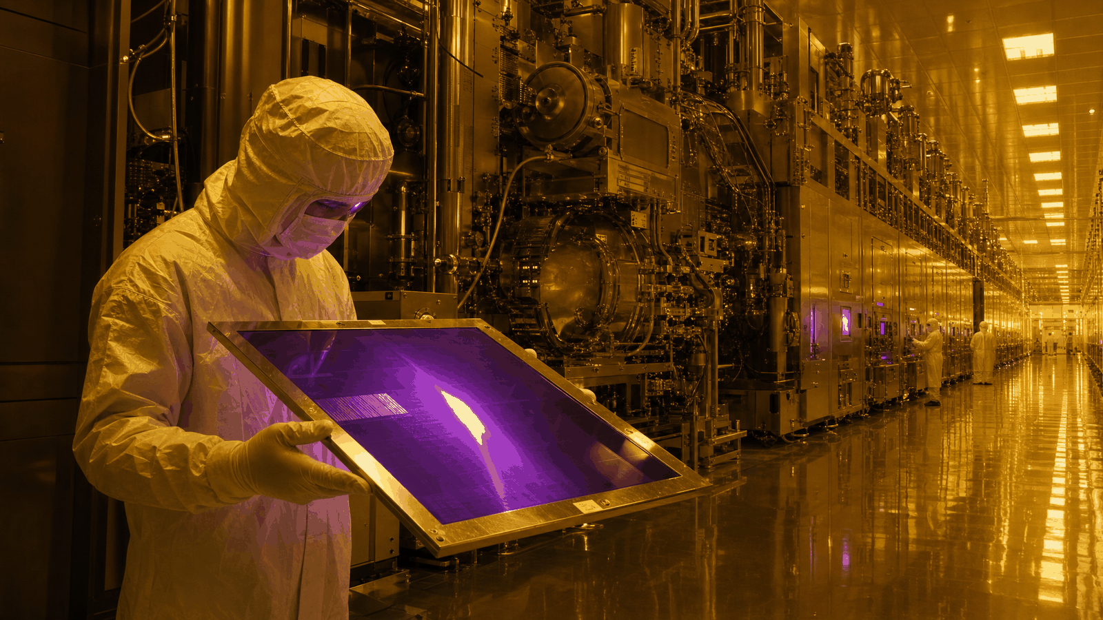
Supply Chained's 2026-09-21 episode covers ASML and TSMC's push toward 12-inch EUV photomasks: why High NA halved throughput, why TSMC waited until 2030, and who will make the mask blanks. Personal listening notes for educational purposes only; not investment advice and not a recommendation of any stock.
Contents
A concave mirror shows things upside down, because there is an obstruction in the middle. The mathematicians call this “the art of the frame.” —— Shen Kuo, Dream Pool Essays, “Disputations I” (Northern Song, c. 1088; my translation)
Shen Kuo used a concave mirror to explain how light crosses at a point and flips the image. More than nine hundred years later, people are still wrestling with the same problem: how to get a mirror to gather more light and shrink a pattern further, without letting the cost eat the gain.
What this episode is about
In the 2026-09-21 episode of Supply Chained, host Tim Culpan and John from the Asianometry channel spend the whole show on one piece of news: ASML and TSMC announced they will work together to move EUV photomasks from 6 inches to 12 inches.
A quick glossary first. EUV is extreme ultraviolet lithography, which uses very short-wavelength light to print circuit patterns onto wafers; every leading-edge chip today depends on it. A photomask is the “negative” for one layer of a chip’s circuitry. In an EUV tool it is a mirror with the pattern on it: light hits it and bounces down to the wafer.
The timeline in the press release: a 12-inch mask pilot line by 2031, 12-inch masks with High NA tools entering production in 2033, and TSMC using High NA in high-volume manufacturing for advanced nodes starting in 2030. John’s first reaction was that TSMC never said it wouldn’t adopt High NA. What it kept saying was that the numbers didn’t work yet.
Key points
1. What High NA is. NA stands for numerical aperture, a measure of how much light the optical system collects. The EUV tools running in TSMC’s fabs today are 0.33 NA; High NA raises that to 0.55, gathering more light and printing finer features. John has seen one in person. He says it’s the size of a school bus, deafeningly loud, and full of gleaming steel pipes, and people call it “the beast.” The roadmap even includes a 0.75 “Hyper NA,” which John puts about 25 years out, with mirrors the size of cars. Tim joked it would need its own small nuclear plant.

2. The price is half the throughput. To accept light at wider angles, the optics had to be redesigned, and the area printed in a single exposure got cut in half. The same wafer needs twice as many exposures, so in John’s words the tool costs twice as much and is now half as productive. Worse, a large chip has to be printed in two halves and stitched together, and the seam is where yield gets lost. TSMC hates stitching.

3. A 12-inch mask wins the area back. A bigger mask restores the full exposure field and removes the stitching constraint. John added an idea of his own: if 12-inch masks could also go into today’s low-NA tools, those older machines might double their output, which both hosts called a monster of a deal. The press release says nothing about this; it’s John’s speculation. It does fit TSMC’s habit of squeezing more out of equipment it already owns.

4. TSMC waited because of cost. TSMC is very good at low-NA EUV, and multi-patterning (printing one layer in several passes) came out cheaper than buying a High NA tool. John recalled Dylan Patel of SemiAnalysis arguing years ago that multi-patterning would stay better until around 2028 to 2030, and TSMC is starting High NA in 2030. Shrinking transistors also doesn’t depend on lithography alone; backside power delivery and gate-all-around transistors are moving forward in parallel. Tim added a practical reason: the fabs are already packed with equipment, so a High NA tool bought today would have nowhere to go.
5. When the two giants move, the industry follows. Mask shops, the Japanese blank suppliers, and chip-design software vendors all have to change. Tim compared it to the move from 8-inch to 12-inch wafers 15 to 20 years ago, when even the pods that carry wafers around the fab had to be redesigned. His line: you’d be pretty stupid not to follow ASML and TSMC down a technology path. He also guessed that TSMC didn’t need customers’ permission, though the technical people at clients like Apple or Qualcomm likely knew this was coming.
6. The hardest gate may be the mask blank. During EUV’s development, everyone assumed the mirrors would be impossible. The light source turned out to be the long pole, and Zeiss spent a decade or more perfecting the mirrors. Defects on a mask blank print straight onto the wafer, so blanks have to be even more perfect than the mirrors, and Japanese suppliers have made them for years. John noticed that no Japanese blank supplier appeared in the announcement, and said ASML and TSMC will have to back a dumpster truck full of cash up to their door. Tim thought that if Japan won’t do it, someone else will, maybe a Chinese company; John answered that there is nobody, since Japan has been doing this for 15 to 20 years. One small detail: on air John wasn’t sure how much bigger a 12-inch mask is. Going from 6 to 12 inches doubles the side, so the area is four times larger, and all of it has to be defect-free.

Further thoughts
The news says a new technology is coming. Will it happen this time?
When I see a headline about a breakthrough, my first instinct is often to get in early. This episode gave me a good counterexample: nobody disputes that High NA works, and TSMC still waited for years.
After listening, I came away with three questions I now ask myself. First, does the cost per unit of output go down? A High NA tool costs twice as much and produces half as much, so the exposure cost per wafer goes up. Second, how much room does the old method have left? Multi-patterning still holds up, so there’s no rush. Third, does the customer have space to install it? The fabs are full. All three answers pointed the wrong way, so waiting was the rational choice.
The timeline deserves a second look too. From the 2026 announcement to 12-inch mask production in 2033 is seven years, and it only counts if mask shops, blank makers, and design software all arrive on schedule. The failure condition I care about most is the blank: if defect rates on 12-inch blanks can’t be driven down, 2033 slides, and that won’t show up in any headline.

Everyone is watching the equipment makers. Could the bottleneck sit in the layer nobody named?
When I look for who benefits, my eyes drift to the biggest, best-known names. When I hunt for bottlenecks, I ask a different question: if demand arrives, which layer breaks first? By this episode’s account, it’s the blank that has to be defect-free, and its suppliers happen to be missing from the announcement.

A bottleneck doesn’t automatically mean profits, though. I kept turning over the line about backing a dumpster truck full of cash up to the door. It means the leaders are willing to pay. It also means the money for new capacity may come from customers, so how much the blank makers keep depends on how the contracts are written and who carries the risk if the scale-up fails. The disagreement between Tim and John matters here too: is the barrier Japan’s 15 to 20 years of accumulated know-how, or could a newcomer skip 6 inches and go straight to 12? John said that’s a startup he’d want to hear about. The signals I’d watch are whether blank makers announce capacity expansions, who funds them, and how prices get set. Until those numbers appear, naming a winner is premature.
References
- Supply Chained, “TSMC, ASML, and High NA EUV,” 2026-09-21
- The ASML and TSMC press release on 12-inch EUV photomasks
- Asianometry’s video series on EUV and lithography
- Shen Kuo, Dream Pool Essays, “Disputations I”
One thing to take with you
Something new being usable and something new being worth it are separated by one number: what each unit of output costs. High NA prints finer lines, yet it doubles the cost per wafer, so the world’s best chipmaker chose to wait.
Here’s something I’ve tried: before upgrading anything, whether a new phone, new software, or a new way of working, I take a sheet of paper and write two lines. The first is “what it lets me produce more of each time.” The second is “how much more money or time it costs me each time.” I only go ahead when I can put a concrete number on both lines. If I can only fill in the first one, I set it aside and look again in a month.
This article is an educational discussion of investment method. It is not advice to buy or sell any individual security, offers no target prices, and does not analyze any current holding. Investing carries risk; make your own decisions or consult a qualified professional.