The Deep Well Inside the Logic Castle — Notes on Asianometry on Whether TSMC Will Make 3D DRAM
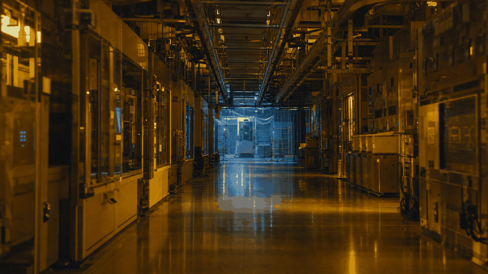
Listening notes on Asianometry, 19 November 2026, "TSMC Making 3D DRAM?": host Jon takes apart The Information's report that TSMC has begun drawing up plans for 3D DRAM at the request of its largest customer, Nvidia. The piece follows how he moves from a packaging reading to a self-fabrication reading, why the DRAM capacitor hole — 1 to 3 micrometres deep and 20 to 30 nanometres wide — implies a new fab, and the failure condition sitting on the oxide-semiconductor path. Educational discussion of research method, not investment advice; no stock recommendations or price targets.
Contents
Custom is a violent and treacherous schoolmistress. Little by little, quietly and unnoticed, she slips in the foot of her authority; and with that mild and humble opening, helped along by time, once she has her position settled she pulls off the mask and shows the tyrannical face underneath. —— Montaigne, Essays, “Of Custom” (1580; my own translation)
Montaigne is describing how people get tied down by their own old rules: when a rule is first set, everyone can state the reason for it, and once it has been in place long enough nobody asks any more whether the reason still holds. A foundry that has stayed away from commodity memory for four decades just got asked a question by its biggest customer, and that reason is what this piece is about.
In the 19 November 2026 episode of Asianometry, “TSMC Making 3D DRAM?”, host Jon discusses reports from The Information and Taiwanese outlets that TSMC, at the request of its largest customer Nvidia, has begun drawing up plans to make 3D DRAM. Jon’s first reading is packaging, since TSMC has been bonding memory and logic wafers since 2023 and in 2025 mentioned bonding 55-nanometre, 6-nanometre and 3-nanometre logic wafers onto memory wafers; then he reads the whole report and overturns himself, because what it says is that TSMC is weighing whether to make the 3D DRAM dies itself. One condition belongs up front: TSMC’s memory revenue share had already fallen below 1% by 2005, and the DRAM capacitor hole — 1 to 3 micrometres deep, 20 to 30 nanometres wide — needs new etching equipment and therefore a new fab, which is why Jon guesses that the self-fabrication path would take 5 to 10 years.
Why doesn’t TSMC make DRAM?
To be precise: TSMC does make memory. It makes embedded memories, cells fabbed alongside logic transistors on the same die — SRAM, embedded DRAM, STT-MRAM, ReRAM, and Jon says the volume on the last of those is not small. What people mean is commodity memory, discrete DRAM or flash sold on its own, and that is Korean territory, unchallenged in any serious way for over a decade.

It has taken those orders before. In the 1990s it made SRAMs and specialty DRAMs for a fabless customer called ISSI; in 1996 it announced with Fujitsu that it would make 16-megabit DRAMs in a new 8-inch fab on a 350-nanometre node, and later 64-megabit parts too. There was no sequel. Fujitsu left the DRAM business in 2002, and TSMC has not signed a DRAM deal of any size since. In both cases it was building a design the customer brought in; with Fujitsu, the Japanese side also shared some of its DRAM manufacturing expertise. By the late 1990s the memory share of revenue was already falling, and the 2005 annual report put it plainly: the company was doing its best to reduce exposure to “commodity memory semiconductor manufacturing services” so as not to be hit by price declines.
Which part of that history hurt the most?
Vanguard. After TSMC spun out of ITRI, ITRI incubated another spinoff meant to make DRAM, the Submicron Project; the government helped fund the purchase of DRAM designs and the construction of an 8-inch fab in Hsinchu, and in 1994 the project was privatised by auction, won by a group led by Dr Morris Chang. TSMC invested in Vanguard directly, the two firms shared top executives, and they went over new fab layouts together.
The start looked promising, and then DRAM crashed. TSMC had to step back in with money and management, and after years of losses Vanguard was ordered out of DRAM and told to make logic chips like its big brother. The same crash crippled the rest of Taiwan’s scattered DRAM industry: a government bailout fell through, Inotera and Rexchip were bought by Micron, ProMOS sold itself to other foundries, and the only independent Taiwanese makers left were Nanya and Winbond, building mature parts like DDR4 and LPDDR4 or niche DRAM at volumes out of all proportion to the leaders. Nanya is the larger of the two and a distant fourth; Jon says that if CXMT had solid numbers, Nanya would probably be fifth. He read Morris Chang’s memoir while researching that episode, and says the bitterness and regret come through.
Two decades have passed, and TSMC’s executives are conservative with long memories. Jon says the Taiwanese have in that time turned building ASICs for customers into a culture, and in conversation they will point out how the business and the temperament differ between logic and memory. Logic means steady profits: no boom like memory, no bust like it either. The customer service, technical understanding and thoughtfulness that foundry demands are what the Taiwanese feel they supply best — and the lengths TSMC will go to for a customer are a strength, I agree with him there. Memory is a commodity, where customers care most about price, and that may not be the game TSMC wants to play; if it does play, it will charge through the nose.
What actually makes a DRAM process different?
Culture is fine, but there has to be a technical reason too, and it comes down to one capacitor.
Fabbing DRAM turns on that vertical cylinder-shaped capacitor, which has to be as tall and skinny as possible: 1 to 3 micrometres deep, only 20 to 30 nanometres wide. The industry calls it high aspect ratio, and etching that hole is said to be one of the hardest things in all of semiconductors. Once it is etched you have to deposit alternating layers of metal, insulator and metal down inside it. TSMC does not do this often, if at all, so it would likely need new etching equipment — and new equipment means a new fab. If it makes memory, it will not be in the existing fabs, and the financial risk goes up a level because of that.

This is the part I most wanted to keep. Two things both called a “process node”, and what separates logic from DRAM is a hole. Outsiders line every fab up by nanometre count, and that line only sorts structures of the same kind.
Packaging, or making the dies?
The passage in The Information is vague: 3D DRAM stacks layers of cells vertically to fit more memory. Jon’s verdict is that the sentence restates what “3D” means.
Start with what supports packaging. The effort is led by a TSMC VP overseeing advanced packaging, Hsu Kuo-chin, and the report adds that he was formerly COO of Micron’s Taichung fabs, so he has memory manufacturing experience too. TSMC has been pushing memory-logic integration since 2023. As for Nvidia: the report says the request came from them, which need not mean they will use it themselves, and Jon’s guess is that they may be asking on behalf of a friend. A startup called d-Matrix has a product it calls 3D-DRAM, stacking compute dies on top of DRAM and connecting them with vertical IO microbumps instead of sitting them side by side on a substrate; done right it brings both capacity and bandwidth, which brings inference economics down. Nvidia and d-Matrix announced a partnership in September 2026, with d-Matrix’s next-generation Raptor XPUs plugging into Nvidia’s AI infrastructure programme. Taiwanese media reported in June this year that TSMC was working with Winbond on wafer-on-wafer stacking, which Jon takes to be some sort of qualification programme.
The clues all point one way, and then the report pushes that explanation aside itself: it states that TSMC is weighing whether to make the actual 3D DRAM dies, possibly by buying an existing fab — the way Micron recently bought one from PSMC — or by building new factories. Jon says he is 100% sure TSMC will not make the commodity DRAM that Samsung and SK hynix make, but he will not rule out a very different new form of DRAM.

If it does go ahead, what path does it have that others don’t?
Oxide semiconductors. A number of TSMC researchers work on them, and they can be turned into something DRAM-ish.
An oxide semiconductor is a device whose transistor channel is made from a special metal oxide instead of silicon. The common one is IGZO, indium gallium zinc oxide; others include indium oxide, indium tin oxide and indium tungsten oxide. IGZO thin-film transistors normally go into displays, and when stackable memory comes up, what people cite is their compatibility with back-end-of-line processing.
The crux is heat. Front end of the line, making silicon transistors, involves thermal oxidation or an anneal to activate implanted dopants, which can reach around 1,000 degrees Celsius; the back end lays down copper interconnects, and copper only tolerates up to 400 degrees. So no more silicon transistors can be made once the back end starts — and traditional 1T1C DRAM needs them. Oxide semiconductors can be produced under those low-temperature conditions, and if that works, many layers of oxide memory cells can be fabricated on top of the silicon ones.

Jon sorts the possibilities into three families. The first and most practical is a straight port of the 1T1C DRAM cell; TSMC researcher Katherine Chiang and her team presented one in June 2025, positioned for last-level cache though it can do more. The second is the capacitor-less oxide gain cell: two transistors, with the data bit stored in the gate of one of them, using the oxide’s ultra-low leakage to hold the charge. IMEC’s Attilio Belmonte has worked on it since 2020, and TSMC and IMEC are close, so what IMEC likes TSMC listens to. TSMC also has an ongoing collaboration with Stanford that has studied various gain cell designs, including ones mixing oxide and silicon transistors. The third is the most exotic, the ferroelectric FET: the gate stack retains a polarization, that stored direction acts on the channel, and the result is a memory cell that is a single transistor with no capacitor — and since the polarization survives power loss, it is nonvolatile. TSMC researchers presented an example in 2023.

All three are stuck on the same thing: reliability. Defects accumulate in the oxide, the transistor’s threshold voltage drifts, and leakage starts rising. Jon calls it a fundamental issue, and says the first company to crack it will win.
So how do I use this myself?
My own worst habit is treating a hard-sounding sentence as a conclusion. “TSMC is going to make DRAM” is exactly that kind of sentence — it gets reposted as a headline — and after this episode my approach is to split it into three layers before deciding whether to care.
The first layer is who is speaking. The Information’s information comes from two people familiar with the matter, with no company confirmation in the report; Jon’s packaging reading and his self-fabrication reading are both his inferences; the papers TSMC researchers have presented are public and checkable. Those three differ a lot in hardness, and reading them together turns “someone is thinking about it” into “it is already happening”. When Jon labels even his own timing estimate as “5 to 10 years sounds sensible to me”, he is doing the same sorting.

The second layer is the gates this has to pass. Does the equipment have to change, does a fab have to be built, does the technology have a failure condition — the episode names all three: new etch tools, a new fab, threshold voltage drift. A story that has to clear every one of those is a long way from paying off, and I can write the gates down as a checklist, so that when one of them moves I know the line is moving.
The third layer is my reason for caring. Jon’s closing section gave me an angle I had not considered: the threat comes from the line between memory and logic melting. HBM4 uses an advanced logic base die, more compute will shift there, and Samsung may be able to use those base dies to improve its own logic process and catch up, or even open a path in compute-in-memory. That would threaten TSMC’s position in logic. Which is why Jon says it cannot sit secure in its logic castle, and that in such a scenario it would have no choice but to make DRAM. The value of that passage is that it rewrites “make DRAM or not” from an opportunity question into a defensive one — and when I read the news I rarely stop to ask whether the subject is attacking or patching a hole.
One more thing: early on, Jon notes that the Jensen situation is still unfolding and then says he is going to shut his mouth, because who knows what happens. I will take him at his word and not speculate.

Further reading
- Asianometry, “TSMC Making 3D DRAM?”, 19 November 2026, host Jon
- The Information’s report on TSMC drawing up 3D DRAM plans (two people familiar with the matter; no company confirmation)
- Asianometry has a separate video on the collapse of Taiwan’s DRAM industry, which Jon recommends himself for anyone who enjoys slow-motion economic car crashes
- Morris Chang’s memoir, which is what Jon read while researching that history
- TSMC’s 2005 annual report and its language on exposure to commodity memory manufacturing services
- The June 2025 oxide 1T1C paper from Katherine Chiang’s team, and the 2023 ferroelectric FET paper from TSMC researchers
- IMEC’s published work on Attilio Belmonte’s oxide gain cells
- d-Matrix’s 3D-DRAM product material, and the September 2026 partnership announcement with Nvidia
One thing to take with you
One idea: a painful failure leaves behind a rule you stop checking. The rule had conditions when it was set — DRAM crashed, the losses ran for years, the bailout fell through, so “we don’t make commodity memory” was right. The trouble is that conditions expire and rules don’t come back to report in. Twenty years later the customers’ needs, the line between memory and logic, and the materials available have all turned over once, and the rule is still standing where it was; because it saved you back then, it is the one you least want to touch.

Something I have tried, and you can do it today: write down one of your current “I don’t do X” rules on paper — avoiding a kind of work, a kind of person, a kind of occasion all count. Next to it write two things: the single event that made you decide that, and the year it happened. Then write one sentence saying whether the condition behind it still holds. Mine was “I don’t start conversations about what I’m working on”, the year next to it was seven years ago, and the person who made me decide that is no longer in my life.
This article is an educational discussion of investment method. It is not advice to buy or sell any individual security, offers no target prices, and does not analyze any current holding. Investing carries risk; make your own decisions or consult a qualified professional.
Comments
Loading comments…