EUV Photomasks Are Getting Bigger: Why One 6×12-Inch Plate Stalled for a Decade
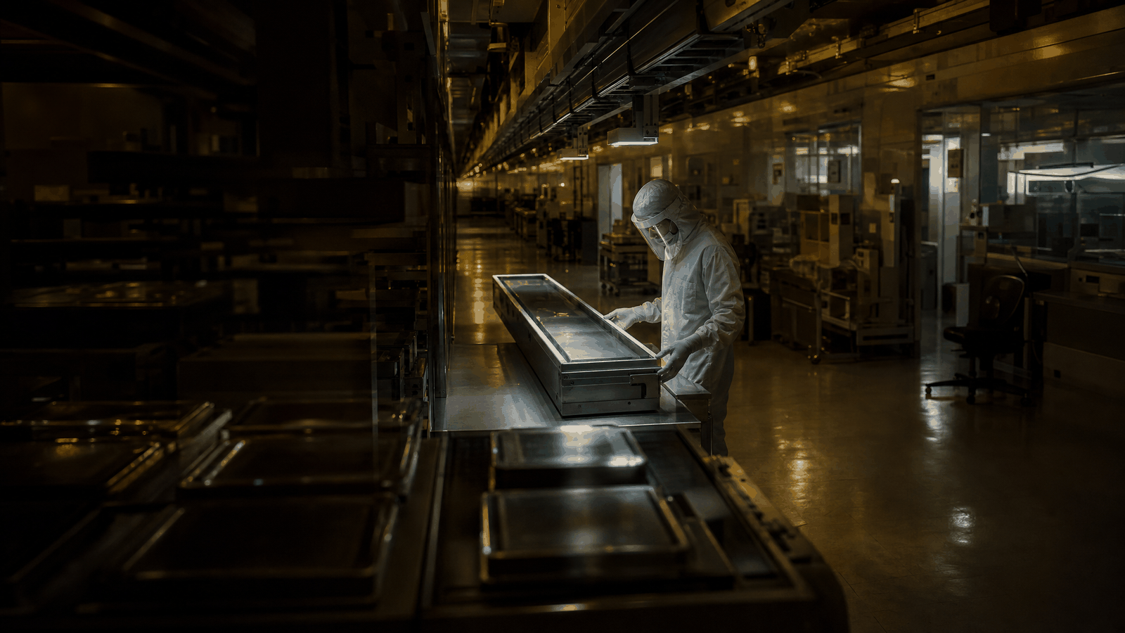
Listening notes on Asianometry's 2026-10-01 episode 'EUV Photomasks Are Getting Bigger.' Working from the TSMC–ASML High-NA timeline, it unpacks why the bigger-mask transition is a cost and coordination problem, and the conditions under which that read breaks. Educational notes on industry structure, not investment advice; no tickers, no price targets.
Contents
- Buying resolution by giving up half the field
- The arithmetic of half a field is worse than it sounds
- How the bigger mask earns the money back
- Where the decade actually went: whoever pays isn’t whoever saves
- The technical problems are real, they just rank second
- The conditions under which this read breaks
- A few other things worth keeping
- Further reading
- The one thing to take away
A clam lay open in the sun, and a snipe pecked at its flesh; the clam snapped shut on the bird’s beak. Said the snipe, “No rain today, no rain tomorrow, and there will be a dead clam.” Said the clam, “You don’t get out today, you don’t get out tomorrow, and there will be a dead snipe.” Neither would let go, and a fisherman came along and took them both.
— Strategies of the Warring States, “Yan II” (compiled by Liu Xiang, Western Han; translation mine)
Asianometry’s episode of 1 October 2026, “EUV Photomasks Are Getting Bigger,” is about something TSMC and ASML announced on the same day: TSMC will put High-NA EUV into high-volume manufacturing in 2030, and to make the arithmetic work, the two of them will push the industry from 6×6-inch photomasks to rectangular 6×12-inch ones, with a pilot line in 2031 and full high-volume production in 2033. The host’s core read is that the technology has been discussed for over a decade while the actual blockage sits in money and coordination — a TSMC senior vice president said publicly in 2024 that the $350 million sticker price on the tool was too high, and bigger masks lift scanner productivity by 23% to 50%, cutting the cost gap against today’s machines in half. The condition: the whole photomask supply chain has to believe it earns the investment back within three to five years.
Buying resolution by giving up half the field
Plain words first. NA is numerical aperture, a dimensionless number for how much light an optical system can collect and focus. Higher NA, finer lines. Almost every EUV machine TSMC owns is a 0.33 NA machine; High-NA takes that to 0.55, bringing half-pitch down to 7.5 or 8 nanometers. That saves expensive multi-patterning, where one layer gets printed in several passes and stacked.
The price shows up in the optics. Raising NA needs bigger mirrors, which makes the light cones bigger, and once those cones interfere with each other the image contrast collapses and the whole exercise loses its point. To avoid the interference while keeping the mirrors at their ideal reflection angles, ASML had to magnify the cones eight times along one of two axes. The exposure field ends up half the industry standard: 33×26 mm becomes 16.5×26 mm.
One shot prints half a design.

The arithmetic of half a field is worse than it sounds
This is where I winced. What took one exposure now takes two, throughput drops, and past a certain point staying on 0.33 NA with multi-patterning is the cheaper option. So when that executive said the sticker price was too high, my own reading is that he was talking about cost of ownership rather than the invoice — $350 million buys you a tool that moves fewer wafers per hour than the old one, and the invoice is the smaller part of the bill.
Chips bigger than the half field, like AI accelerators, make it worse. You have to stitch exposures A and B together. imec, ASML and everyone else has papers saying stitching can be done, but the host describes the look on the faces of TSMC people when he brings up stitching as the same look he makes when his dad tells him he should lose a few kilograms. Chip designers dislike it too, because the seam rams a Korean DMZ through the middle of their design.

Worth pausing here: ASML had no third option. Better resolution meant either accepting the smaller field or getting the industry onto a bigger mask. And when High-NA was being planned over a decade ago, the mask makers said they would not go bigger without an explicit commitment from the chipmakers, while the chipmakers would not commit to that investment before they had even deployed low-NA EUV. Both positions hold up on their own, and ten years went by. There is no fisherman in this story, but the waiting ended the same way it does for the snipe and the clam.
How the bigger mask earns the money back
A 6×12-inch mask restores full-field exposure for High-NA. Per Intel, scanner productivity rises somewhere between 23% and 50%; the host bets on the upper end, which halves the cost gap. Stitching goes away, and design flexibility comes back. ASML’s CEO called it a no-brainer publicly back in October 2024 — the hard part being to get everyone else to go along with the no-brainer.
One detail I enjoyed: ASML left only 11.2 inches of travel space inside the reticle chamber, so the real size is 6×11.2 inches. It works because the 33 mm field times eight magnification is 10.4 inches, which fits. The industry will keep saying 6×12 anyway, and the mixed imperial units are a historical artifact; the host asks not to be yelled at in the comments about it.
An extension worth holding onto: once the bigger masks exist, ASML will put them on 0.33 NA machines too. A 6×12 mask at 0.33 NA means twice the real estate — a larger AI chip, or the same design duplicated to print at twice the speed. One estimate has a low-NA machine with the bigger mask patterning 450 wafers an hour or more, with the three-pulse light source on top of that.

Where the decade actually went: whoever pays isn’t whoever saves
Reading the news invites a mistake: if the arithmetic works, surely the industry moved already. What I took from this episode is the habit of asking who the arithmetic was done for.
For a wafer fab, the change is the scanner plus the gear for mask handling, inspection and stocking. Not trivial, and the rest of the fab is untouched.
For a mask shop, everything changes. Look only at reticle handling: pod stockers, pod cabinets, pod washers, pod inspectors, the overhead hoist transports carrying the pods — all of it. They may have to rebuild the shop, running new and old lines side by side for a while, because not every customer will pay up for bigger masks. Current estimates put the new tooling at 20% to 100% more than its 6-inch ancestors.

And a mask shop is not an end-to-end factory. The host’s analogy is a sushi chef: the chef assembles the sushi and serves it, but he isn’t catching the fish, he buys it. EUV mask blanks come from AGC and Hoya in Japan; pellicles from Mitsui Chemicals or the Finnish firm Canatu; protective pod carriers from Entegris in the US and Gudeng Precision in Taiwan; mask writers from IMS or NuFlare; etchers and cleaners from Applied Materials and Shibaura; actinic defect inspection from KLA or Lasertec; repair and optical verification from Zeiss. The list goes another layer down into those companies’ own suppliers.

So “switch to bigger masks” needs a large share of that list to sign at once, each one spending real money upfront on the belief that it returns in three to five years. Which is what Samsung heard in 2024 when it polled its suppliers about blanks for larger masks: the answers clustered on industry consensus, appropriate and open standardization, and business drivers, rather than on any unbeatable technical wall.
The technical problems are real, they just rank second
The engineering list exists. Can the multilayer hold the same performance over twice the area, reflecting the 13.5-nanometer central wavelength evenly across the whole mask. For compatibility the bigger mask has to keep the same 0.25-inch thickness as the old 6×6 while weighing nearly twice as much, which raises sagging in the middle and physical stress during handling. Then the High-NA-specific items: stitching, anamorphic exposure, and the curvilinear revolution with its curvy-line masks and inverse lithography, a leap that hasn’t fully landed yet.
I’d still say these look like problems with answers, because people are already spending money. Gudeng moved fast to work the standards bodies at SEMI and get its RSP 612 carrier written into spec — once you’re in the spec it’s very hard to get pulled out — and published a paper on what a bigger mask does inside the carrier, running computational fluid dynamics on the stresses on the reticle and the movement of purge gas. Another firm making transporters for critical semiconductor materials already lists a 6×12-inch carrier on its website. AGC has started producing larger prototype blanks; investors have been sniffing around since mid-2024 while the company kept its usual silence, and Intel mentioned in a 2025 talk that it had received AGC prototypes along with other ecosystem items. Intel has championed large masks since 2023 and has been open about working with partners and sharing what it learned, which the host gives them credit for.
TSMC and Samsung issuing releases the same day moves this from one company wanting it to the industry being on board.
The conditions under which this read breaks
This is the part I care about most. How literally should anyone take a roadmap five years out? What I do now is check three things.
First, whether the payback holds. EUV mask sets already cost tens of millions of dollars. Per a 2025–2026 economic projection from Micron, an EUV mask set costs six times a regular optical set and lasts a fifth as long, and the number of masks in a set keeps rising. Who pays? The foundries and their customers — the AI chipmakers like Nvidia and AMD, maybe OpenAI or Anthropic. If any link decides three to five years won’t do it, the timeline slips.
Second, concentration. This is a subset of a subset of an industry, and virtually everything is single-sourced. One technical mess-up or supply problem at any major player can push the whole thing out.
Third, whether the demand is still there in five to seven years. The host says the EUV market right now is about as hot as an EUV photomask during exposure — masks heat to 35–50°C under that light, which is why they’re built on low-thermal-expansion glass. Will it still be that hot when the big masks hit the fab floors? Nobody knows. Given how fast AI moves and how old the boom is, the reasonable guess is that the world looks different by then. His read: TSMC gave itself five to seven years because once the commitment is public, it has to hit the date no matter what the economy looks like.
Together those three gave me a test I can carry to other industries: check whether the roadmap puts the cost on someone else, whether third parties have already spent money on visible things (prototypes, standards, carriers), and whether a competitor endorsed the timeline on the same day. When all three hold, I take it seriously. When only the first one holds, it’s usually a wish list.
A few other things worth keeping
- How a mask blank is made: start with ultra-flat low-thermal-expansion glass, polish it using surface-shape measurement to locate the spots that need local work; deposit 40 alternating molybdenum-silicon pairs about 7 nanometers thick each by ion beam deposition, spinning the substrate and varying both the beam angle on the target and the substrate tilt for uniformity; add an insulating dielectric layer (silicon dioxide or ruthenium) as a buffer and etch stop; add an absorber layer, perhaps tantalum, to eat the radiation and stop reflection; cover the surface with a silicon or carbon-nanotube pellicle against particles; coat the back of the glass so an electrostatic chuck can hold it.
- Getting one defect-free blank is doable, twice or a few times too. The hard part is a process that delivers that perfection at high volume.
- That electrostatic chuck, the host notes, may be made by Toto, the toilet maker. Semiconductor supplier lists read like this more often than you’d think.
- It’s early — five to seven years of runway. Expect more prototypes in the coming years.

Further reading
- Asianometry, “EUV Photomasks Are Getting Bigger,” 1 October 2026
- TSMC and ASML’s public statements of 1 October 2026 (Samsung issued its own the same day)
- Intel’s public sharing on large masks since 2023
- SEMI reticle carrier standards documents (RSP 612 and related)
- Micron’s 2025–2026 photomask cost projection
- imec’s High-NA resolution results
The one thing to take away
When something makes sense on paper and still doesn’t move, go look at whether the cost and the benefit land on the same person. The arithmetic describes a system; the button gets pushed by whoever has to pay first. The bigger mask’s benefit lands in the wafer fab and the spending lands in the mask shop, and so a decade went by.
Something I’ve tried: take one thing at home or on your team that’s been discussed for six months without moving, draw two columns on a sheet of paper, and write on the left who pays — money, time, hassle, things they’d have to relearn — and on the right who collects the benefit. If the names differ, your next step is to find the person on the left and ask what it would take for them to move.
This article is an educational discussion of investment method. It is not advice to buy or sell any individual security, offers no target prices, and does not analyze any current holding. Investing carries risk; make your own decisions or consult a qualified professional.